AMD’s announcement of its fourth generation EPYC 9004 Series processors includes major advances in how these chipsets are designed and produced for delivering the highest performance levels. These advances involve using a hybrid multi-die architecture.
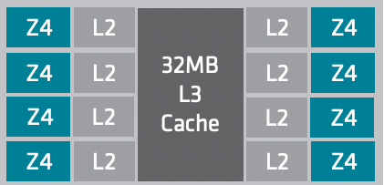
This architecture makes use of two different production processes for cores and I/O pathways. The former makes use of five nanometer dies, while the latter uses six nanometer dies. Each processor package can have up to 12 CPU dies, each with eight 8 cores for a total of 96 cores in the maximum configuration. Each eight-core assembly has its own set of eight 8 dedicated 1 MB L2 caches, and the overall assembly can access a shared 32 MB L3 cache, as shown in the diagram below.

In addition to these changes, AMD announced improvements called Zen 4 that involve boosting instructions-per-clock counts and overall clock- speed increases. AMD promises roughly 29 percent faster single-core CPU performance in Zen 4 relative to Zen 3, which were affirmed with Ars Technica’s tests earlier this fall. (Zen 3 chips used the older seven 7 nanometer dies.)
This configuration provides a great deal of flexibility in how the CPU, memory channels, and I/O paths are arranged. The multi-die setup can reduce fabrication waste and offer better parallel processing support. In addition, AMD EPYC processors are produced in single and dual socket configurations, with the latter offering more I/O pathways and dedicated PCIe generation 5 I/O connections.


